Implementing the Instruction Controller
- Anthony Faulise
- Apr 18, 2025
- 6 min read

Before I dig in:
As I was doing the circuit design, I made some observations that call for more revision of past decisions. Sorry, that’s just the way design goes. You lay something out, later reality points out an impracticality, you revise.
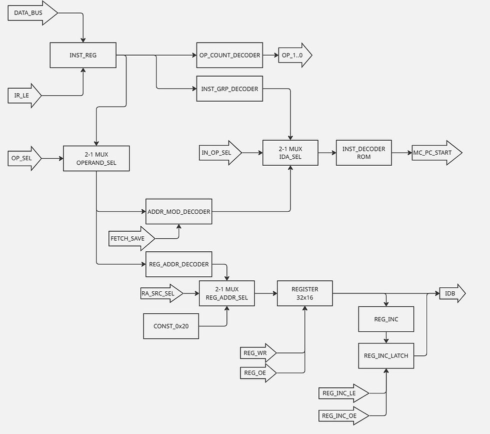
Also, I kind of realized that the Instruction Controller was over-reaching into the domain of the MicroCode lookup and MicroCode Sequencer. I’m going to reduce the boundary of the Instruction Controller so that it sends the MicroCode Start address and MicroController Start signal to a separate block. Here’s the reduced block diagram:
Instruction Group Mapping - ReDo
As I was designing the Instruction Group Decoder circuit, I realized there are four cases when the low 4-bits of the Instruction Decoder Address have to be driven by different bit-fields of the IW:
2-operand
1-operand
0-operand
Special-group instructions.
This clearly calls for a 4-1 multiplexer to map different parts of the IW to the low bits of IDA. Unfortunately, I assigned the Instruction Group IDs for these four cases as 001, 010, 011, and 100.
I could build some logic to map these to 00, 01, 10, and 11. Or, I can just redefine IDA6-IDA4 so that just two of the three bits are needed to drive a multiplexer directly. To do that, I need to re-map the Instruction Group for “Fetch Operand” to a different Instruction Group ID. So, I have to change some of the tables in previous posts. Sorry if this generates confusion.
Here’s the result:
Lookup Type | IDA6-IDA4 | IDA3-IDA0 |
Special 0-Operand | 000 | (Logic Mapping) |
2-Operand Instruction | 001 | IR15, IR14, IR13, IR12 |
1-Operand Instruction | 010 | IR9, IR8, IR7, IR6 |
0-Operand Instruction | 011 | IR3, IR2, IR1, IR0 |
Operand Fetch | 100 | 0, MLB2, MLB1, MLB0 |
Result Save | 101 | 0, MLB2, MLB1, MLB0 |
Unused | 110 | n/a |
Reserved | 111 | (Logic Mapping) |
Looking more closely at how the IW influences ID6-ID4:
Instruction Word | Instruction | ID6-ID4 | Instruction / Instruction Group |
1111 0 dddddddd ccc | BRA | 000 | Special |
1111 100000 mmmmmm | IM | 000 | Special |
1111 100001 mmmmmm | SWI | 000 | Special |
1111 100010 000ccc | JMP | 000 | Special |
1111 100011 000ccc | JSR | 000 | Special |
0000 aaaaaa bbbbbb to 1110 aaaaaa bbbbbb | LD, ADC, ADD, AND, CMP, OR, SUB, SBC, XOR | 001 | 2-operand instructions |
1111 110000 bbbbbb to 1111 110111 bbbbbb | NOT, NEG, INC, DEC, ROT*, SHIFT* | 010 | 1-operand instructions |
1111 111111 00 0000 to 1111 111111 00 1111 | RTS, SWI, RTI, NOP, STC, CLC, etc. | 011 | 0-operand instructions |
Using a Karnaugh map, I derive these equations to produce ID6-ID4:
ID6 = 0
ID5 = ((IW15-IW12) and IW11 and IW10 and NOT IW9) OR
(AND(IW15-IW12) and IW11 and IW10 and IW9 and IW8 and IW7 and IW6 and NOT IW5)
IW4 = NOT(AND(IW15-IW12)) OR
AND(IW15, IW14, IW13, IW12, IW11, IW10, IW9, IW8, IW7, IW6, NOT IW5)
If I reassign the mapping for OP1 and OP0 as follows, I can even recycle the ID5 and ID4 bits to drive OP1 and OP0, saving some logic:
Instruction Group | OP1, OP0 |
Special | 00 |
2-operand | 01 |
1-operand | 10 |
0-operand | 11 |
OP1 = ID5
OP0 =ID4
Finally, I realized I made a minor mistake with mapping the ID3-0 bits for Special instructions. I left the bits undefined for BRA instruction. Here’s the fixed table.
Instruction Word | Instruction | ID3-ID0 |
1111 0 dddddddd ccc | BRA | 0100 |
1111 100000 mmmmmm | IM | 0000 |
1111 100001 mmmmmm | SWI | 0001 |
1111 100010 000ccc | JMP | 0010 |
1111 100011 000ccc | JSR | 0011 |
Here’s the logic for Special Instructions when ID6-4 = 000:
ID3 = 0
ID2 = AND(IW15, IW14, IW13, IW12, not IW11)
ID1 = AND(IW15, IW14, IW13, IW12) AND (IW11, not IW10, not IW9, not IW8) AND IW7
ID0 = AND(IW15, IW14, IW13, IW12) AND (IW11, not IW10, not IW9, not IW8) AND IW6
Back to the Instruction Controller Design
I used Logisim-evolution to design and simulate the circuitry, not based on extensive research but because it was free and came up near the top of my Google search.
To keep the circuit diagram from becoming too complex, I used Logisim’s “Subcircuits” ability to design each of the functional blocks in my block diagram in a separate Logisim tab and then glued them together with data busses.
I chose to design the master controller as a Moore state machine, meaning the outputs are determined only by the current state. I did this because the states are used primarily to track what should happen next, rather than to condition the response of the system to current inputs. The current state ID plus the inputs determine what the next state ID will be, though. On every clock transition, the next state is latched from the state lookup table output to the data latch and determines the new current-state.
Let’s work through each of the major sections:
Instruction Group Decoder
Addressing Mode Decoder
Register Address Decoder
Operand Selector
Register Address Selector
Instruction Decoder Address Selector
Register Incrementer and Latch
Then I’ll weave them all together.
Operand Count Decoder
I realized I could just use the IDA bits 5 and 4 for this, so I no longer need a separate circuit.
Instruction Group Decoder
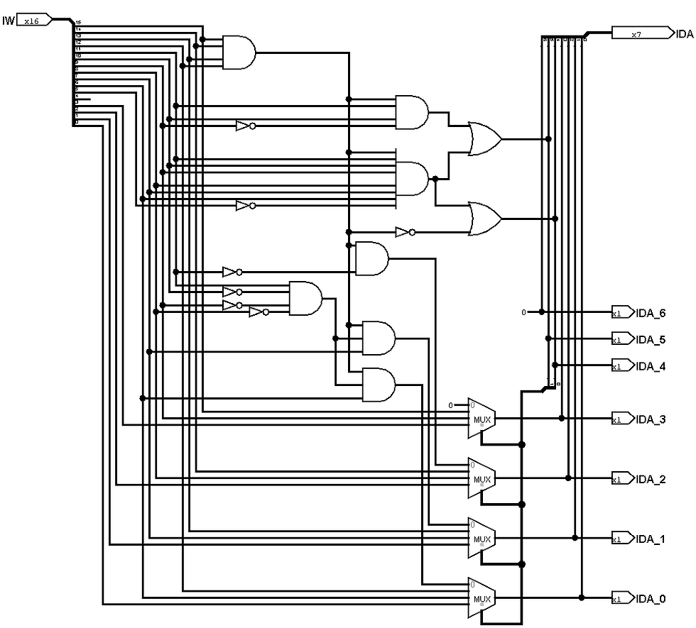
At the top, we use glue logic to implement the decoding of the IW and generation of IDA_6, IDA_5, and IDA_4. Note that IDA_5 and IDA_4 also serve as OP_1 and OP_0. Note that a 12-input AND gate would be required in the top section, something that isn’t available as a discrete component. I chose to cascade a 4-input AND of the top 4-bits of the IW, since that is an intermediate term that can be reused in several other parts of the circuit. This structure adds a gate delay to the production of the IDA output, but seems worth it.
In the middle section, we extract the relevant fields of the IW for use in the Special instructions and route those bits to the low-bit multiplexers.
In the lower section, we see multiplexers used to route sub-fields of the IW to the lower-four bits of the IDA. For Special instructions, the data come from the mapping function in the middle of the circuit diagram. Note that bits IDA_5 and IDA_4 are used to drive the select inputs of the multiplexers.
Addressing Mode Decoder
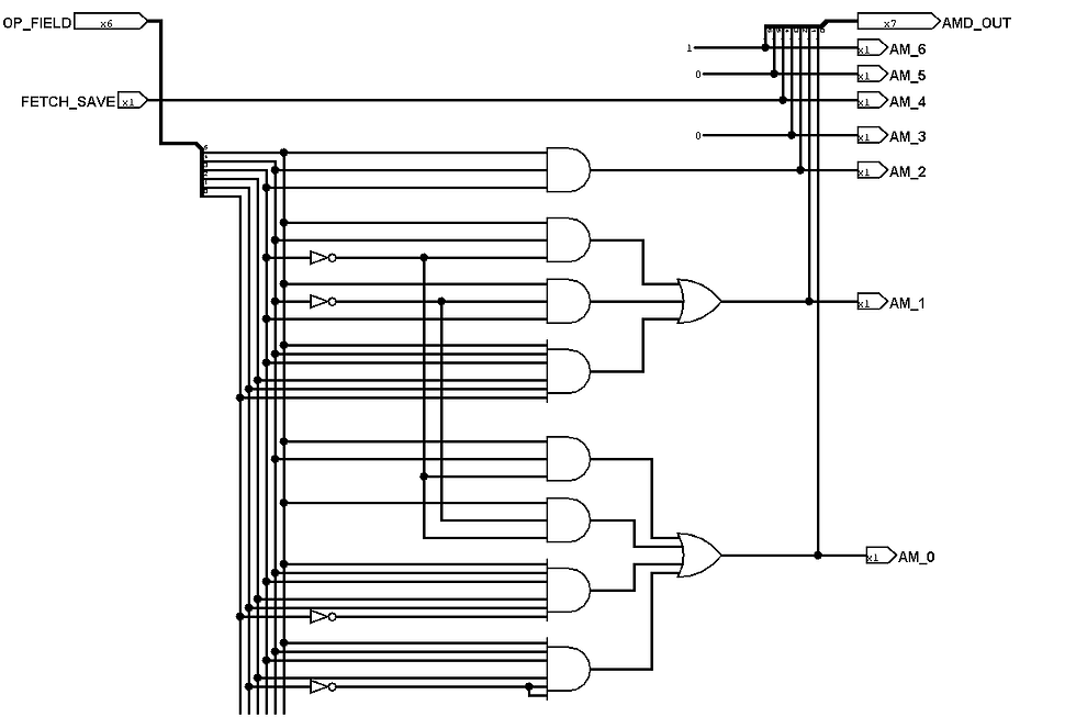
This is a straightforward NOT-AND-OR implementation of the logic equations specified earlier.
Register Address Decoder

This is a straightforward NOT-AND-OR implementation of the logic equations specified earlier, used to generate the addressing bits to select the correct register based on the addressing mode and operand-select bit-fields.
Operand Selector
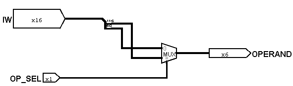
Here we route bits 5-0 and 11-6 from the Instruction Word to a 2-1 multiplexer driven by the OP_SEL signal. This circuit selects which operand within the IW should be routed to the Addressing Mode decoder and the Register Address Decoder.
Register Address Selector
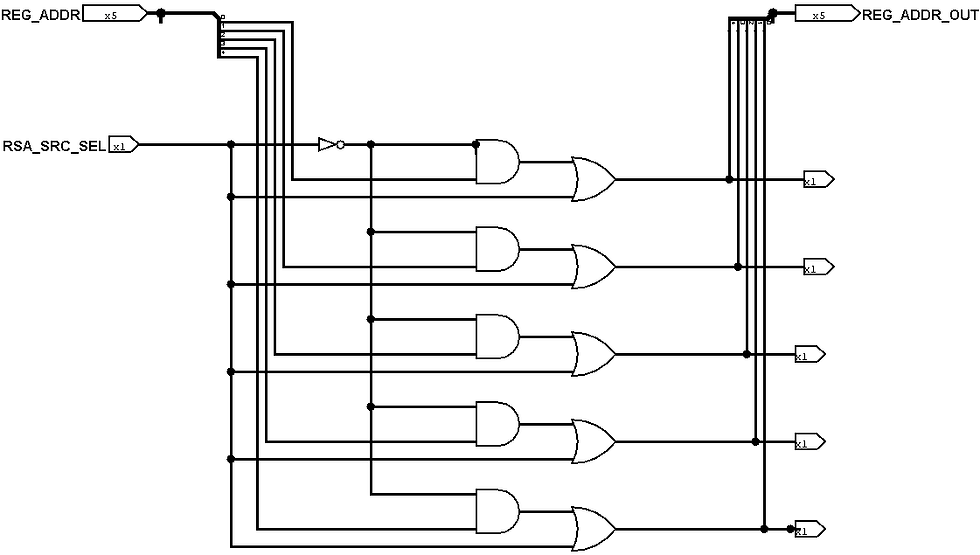
The Register Address Selector either passes the Register Address input to the output when RSA_SRC_SEL signal is low, or forces REG_ADDR_OUT to 0x1f when RSA_SRC_SEL is high. This is used to forcibly select the PC when the IC is incrementing the PC during the instruction cycle.
Instruction Decoder Address Selector
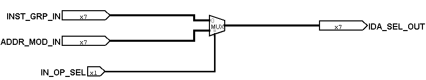
This circuit simply selects whether the Instruction Group Decoder or the Addressing Mode Decoder output should be routed to the Instruction Decoder lookup ROM, according to control by the IN_OP_SEL (Instruction / Operand Select) input.
Register Incrementer and Latch
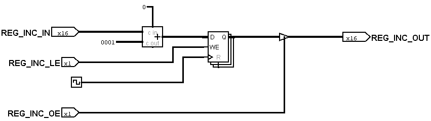
This circuit adds 0x01 to the current REG_INC_IN value and captures the value with a latch, then controls the output with an Output Enable signal. In practice both the REG_INC_IN and REG_INT_OUT words will be connected together at the Internal Data Bus.
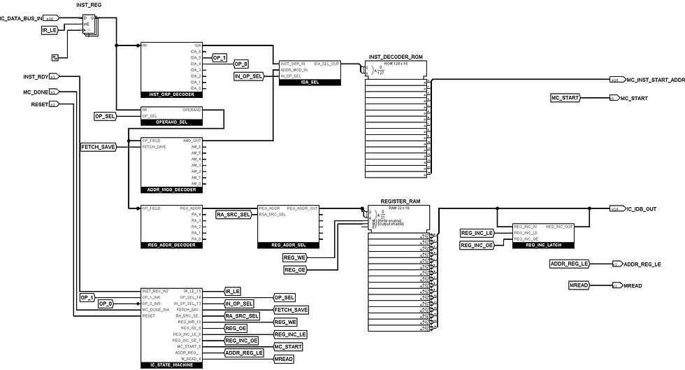
Bringing it All Together
The diagram below shows all of the foregoing blocks, plus the Instruction Decoder ROM and a Register RAM. The IC_STATE_MACHINE is a straightforward Moore state machine that could be implemented with logic (4-bits input, 12-bits output + 4 bits state) and a 4-bit register to store the current state. I expect I should be able to implement it with one or two 22C10s depending on how creative I am.
It all seems to work in simulation…
To really test everything, I’ll need the MicroSequencer circuit so I can tie the two together. Even with the MicroSequencer, I’ll have to manually simulate the bus controller to provide instruction and operand reads and writes, but those are expected to be slow for now and not timing dependent.
So, my next step is to plan, design, and implement the MicroCode Sequencer!


Comments